High-voltage inspection · Application note
X-Ray Inspection of High-Voltage Power Supplies and Power Modules
- Published 13 October 2026
- 19 min read
- Curpow application engineering
Short answer
High-voltage assembly inspection needs resolution in the tens of micrometres, enough kV to cross the case and the copper behind it, and contrast at the void. The CX30 reaches 130 kV and publishes its full spot against power curve. The CX20 runs to 110 kV at 25 W, and the CX40 holds the smallest spot at 4.5 µm.
On this page
- What X-ray inspection finds inside a sealed high-voltage assembly
- Potted supplies, high-voltage modules and power modules: What changes for inspection?
- In-line radiography and lab CT for high-voltage assemblies
- What resolution high-voltage assembly inspection needs
- How focal spot size changes with tube power
- Tube voltage and contrast through potting and a case
- Spot position stability for CT reconstruction
- Choosing between the CX20, CX30, and CX40 for high-voltage assembly inspection
- Lead time and second sourcing
- How to specify an X-ray source for high-voltage assembly inspection
- What this means for your source selection
- Sources
Manufacturers fill a high-voltage power supply with a resin that sets hard around the parts inside. The resin stops the voltage jumping across the gaps in there. Once the resin sets, nobody can open the unit to look inside without wrecking it. So manufacturers use an X-ray machine to check that the resin reached every gap and left no air pockets behind. Curpow builds the X-ray sources that go inside those machines.
Researchers have already measured what an air pocket costs: the voltage at which a void inside epoxy starts to discharge, and the temperature a chip reaches once voids block its heat path. We took those published numbers, added what the automotive qualification guideline requires a manufacturer to record, and checked the CX20, CX30, and CX40 against them. So you can read the requirements and our specifications in the same place.
Manufacturers use X-ray to find voids in the potting, voids in the solder under a die, delamination at an encapsulant bond, and parts that shifted during casting. Four things decide whether an X-ray source suits this work. Contrast at a small air gap inside a light compound. Focal spot size at the power you actually run. Enough kV to cross the case and the copper behind it. Spot position stability, if you are reconstructing. This page works through each one.
Key takeaways
- An air pocket inside a high-voltage assembly is the defect that ends its life. In a cast resin transformer insulation model, voids from 0.21 mm to 0.65 mm across produced partial discharge of 5 pC to 28 pC, rising with void diameter. A void in a solder layer blocks the heat path out of a die. Both sit under a compound that nobody can cut away without destroying the unit.
- Potted supplies and power modules load the beam differently. Epoxy and silicone are light, so a cast assembly gives up its interior easily. A power module puts a 3.00 mm copper substrate in the beam path, and the copper decides the tube voltage.
- Contrast decides more of this work than penetration does. A void in potting is a small density step inside an already light material. Raising kV gets you through the case and flattens that step at the same time, so check contrast at the compound rather than reading the kV number alone.
- Run radiography to screen and CT to adjudicate. One exposure gives you a density map of a whole joint area in seconds. Reconstruction measures a void’s size, shape, and position instead of estimating them by eye, and reconstruction costs scan time.
- Ask for the focal spot at the power you will actually run. The CX30 spot measures 8 µm at 4 W and 60 µm at 40 W. Most data sheets publish one best-case figure, so a single minimum spot number tells you little about your duty cycle.
- The CX20, CX30, and CX40 each suit a different part of this work. The CX30 reaches 130 kV and publishes its full spot against power curve. The CX20 runs to 110 kV at 25 W. The CX40 holds the smallest spot in the range at 4.5 µm.
What X-ray inspection finds inside a sealed high-voltage assembly
A cast or potted assembly is closed for good. Cutting one open destroys the part and the evidence together. So manufacturers use X-ray to see inside instead. It finds five kinds of defects:
- Voids in the potting around a high-voltage termination. Air has a relative permittivity near 1. Cast epoxy sits between about 3.5 and 4.5. So the field across an air-filled void runs several times higher than the field in the resin around it. Once that local field passes the breakdown strength of air, the void starts to discharge. Partial discharge erodes the resin wall from the inside, and the erosion runs until the insulation fails. Published work on cylindrical voids enclosed in epoxy and mica measured that inception voltage from 0.1 Hz to 300 Hz and from 20 °C to 155 °C. The inception voltage depends on both.
- Voids in the solder or sintered layer under a die. The solder under a chip is the primary heat path out of that chip. Inspection work on EV power modules puts those layers at under 100 µm thick. Air conducts heat poorly, so heat cannot cross a void and has to travel sideways through the solder and around it.
- Delamination where an encapsulant has let go. A bond between an insulation layer and its encapsulant can fail without opening a visible gap on the outside. CT work on solid dielectric switchgear, underground terminations, transformer bushings, and encapsulated junctions names delamination and voids in epoxy potting as its target findings.
- Component placement and internal geometry. A multiplier stack, a transformer, or a creepage barrier that shifted during casting stays exactly where the resin set it. Radiography shows where each part ended up against where the drawing puts it.
- Contaminants and foreign objects. A metal fragment cast into the resin sits at a much higher attenuation than the compound around it, so it shows up as a bright inclusion.
The automotive qualification guideline AQG 324 requires manufacturers to record void, delamination, and crack formation in solder, diffusion solder, and sintered interconnections, and for that examination it recommends scanning acoustic microscopy. The same guideline lists X-ray alongside acoustic microscopy in its module test set. For flaws, cracks and deformation in potting and sealing materials, it names X-ray, CT, acoustic microscopy, and micro-sections together. Acoustic microscopy reads the bond planes. X-ray images the whole assembly in one exposure, which is how one station also catches potting voids, shifted components, and metal contaminants.
| Feature | Reported dimension | What was measured, and when | What it does not show |
|---|---|---|---|
| Chip solder layer thickness | 0.10 mm | Seven-layer IGBT module model, 1200 V/50 A device, finite element study, 2023 | A modelled stack rather than a measured production part |
| Substrate solder layer thickness | 0.20 mm | Same model | Same |
| Copper substrate thickness | 3.00 mm | Same model | Nothing about potted supply housings |
| Silicon die thickness | 0.32 mm | Same model | Same |
| Void fractions studied in a solder layer | 3.9 percent to 34.9 percent, from cylindrical voids of 0.5 mm to 1.5 mm radius | Same model | No occurrence rate in production |
| Void fraction where junction temperature climbs steeply | 7.6 percent, at a void radius of 0.7 mm | Same model | Not a pass or fail limit, and a simulation result rather than a measurement |
| Solder layers in EV power modules | Often under 100 µm | Described by an inspection laboratory from its own EV module work | Not a published specification |
| Void diameter in a cast resin insulation model | 0.21 mm to 0.65 mm | Epoxy moulded electrode, brass parallel plate electrodes 25 mm across at a 3 mm gap, 2012 | A laboratory model, not a production transformer |
| Partial discharge charge from a void in that model | 5 pC to 28 pC, rising with void diameter | Same model, measured under X-ray irradiation | The study irradiated the sample to trigger discharge rather than to image the voids |
| Voids in epoxy potting around a high-voltage termination | Found by CT, one example scanned at 25 µm | High-voltage components at an accredited inspection laboratory | No void dimensions published |
Module stack, void fractions, and junction temperature from Xu et al. 2023; cast resin void diameters and discharge charge from Higashiyama et al. 2012; solder layer thickness in EV modules from XRAY LAB; potting voids and delamination from Nel PreTech; void inception voltage in epoxy from Aakre et al. 2020; interconnection layer requirements from ECPE Guideline AQG 324 Release 04.1/2025. Full references at the foot of the page.
Potted supplies, high-voltage modules and power modules: What changes for inspection?
The assembly decides two things that matter to a source: how much material the beam has to cross, and how hard the defect is to separate from the material around it.
| Assembly | Construction | What the beam crosses | What that means for the source |
|---|---|---|---|
| Potted high-voltage supply | A transformer, capacitors, and a multiplier stack cast into epoxy or silicone, closed in a case | A light compound, plus copper windings and the case wall | The compound gives up its interior easily, so the windings and the case set the tube voltage. The void is a small density step inside a light material, so contrast decides whether you see it |
| High-voltage module | A smaller cast block with fewer dense parts inside it | Less compound and less copper than a full supply | The shortest path of the three. A source that handles a full potted supply handles a module comfortably |
| Power module with a copper baseplate | A silicon die 0.32 mm thick, chip solder 0.10 mm, direct bonded copper on alumina, substrate solder 0.20 mm, and a copper substrate 3.00 mm thick | Copper, ceramic, copper, solder, and more copper in series | Copper sets the tube voltage here, not the compound. Beam hardening through the copper distorts contrast if you do not tune the exposure to this stack |
Power module stack from Xu et al. 2023, a finite element study of a 1200 V/50 A device. Beam hardening through copper from XRAY LAB. Potted assembly construction described from the high-voltage component types listed by Nel PreTech.
In-line radiography and lab CT for high-voltage assemblies
Radiography takes one exposure and gives you a density map of the full joint area in seconds, with voids appearing as lighter regions. That is fast enough to screen every unit coming off a line. But one image lays the whole assembly on top of itself. You can see that a void is present. You cannot tell which layer it sits in, or how deep it runs.
CT reconstructs the assembly in three dimensions, so an operator measures a void’s size, shape, and position instead of estimating them by eye. On a multi-layered power module that separation matters, because the solder layers stack directly above one another and one image cannot tell them apart. CT work on solid dielectric switchgear and transformer bushings scans at 25 µm.
The trade is scan time against certainty. Use radiography to screen production and CT to qualify a design, investigate a failure, or judge a borderline unit.
| Method | Reported result | What was measured, and when | What it does not show |
|---|---|---|---|
| 2D and 2.5D radiography | A density map of the full joint area in seconds, with voids appearing as lighter regions | Described by an inspection laboratory from its own EV power module work | Which layer a void sits in, or how deep it runs, from a single perpendicular image |
| CT | The joint reconstructed in three dimensions, so an operator measures void size, shape, and position rather than estimating them | Same laboratory | Anything at line rate |
| CT of high-voltage components | Delamination, voids in epoxy potting around a high-voltage termination, warpage, and contaminants. One example scanned at 25 µm | Solid dielectric switchgear, terminations, sensors, and transformer bushings at an accredited laboratory | No published void dimensions or acceptance limits |
Radiography and CT capability from XRAY LAB; high-voltage component findings and the 25 µm scan from Nel PreTech.
What resolution high-voltage assembly inspection needs
High-voltage assembly inspection needs resolution in the tens of micrometres, not single micrometres. The voids that end a high-voltage assembly’s life measure hundreds of micrometres. An epoxy moulded electrode built to model cast resin transformer insulation carried voids from 0.21 mm to 0.65 mm across, and the discharge rose from 5 pC to 28 pC as the void diameter grew. In a modelled IGBT stack, the junction temperature starts climbing steeply at a void radius of 0.7 mm. Inspection work on EV power modules puts the threshold manufacturers flag at roughly 10 to 15 percent of joint area, though the threshold varies by module design and duty cycle.
The feature holding the void sets the resolution floor, not the void itself. Solder layers in EV power modules often run under 100 µm thick, and a chip solder layer in a modelled IGBT stack measures 0.10 mm. CT work on solid dielectric switchgear and transformer bushings scans that class of component at 25 µm.
So resolution does not usually fail you on this application. A microfocus source in the 4.5 µm to 7 µm range clears the requirement with a large margin. You spend that margin on flux when your cycle time needs it.
How focal spot size changes with tube power
Tube power drives focal spot size. The spot is where the beam current lands on the target, and the target has a thermal limit. More power has to spread over more area. That means a data sheet quoting a minimum focal spot and a maximum power output is quoting two numbers that do not occur together.
Curpow publishes the full relationship on the CX30 rather than a single best-case figure. That is the only way to answer the question an integrator actually has: what is the spot at the power my line needs?
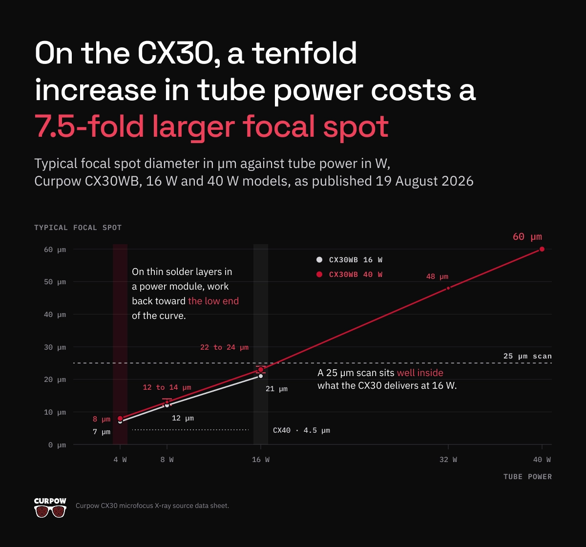
Read down the 40 W column and the shape of the trade is clear. Power rises ten times, from 4 W to 40 W. Spot diameter rises 7.5 times, from 8 µm to 60 µm. Because spot area goes as the square of diameter, the area grows about 56 times, so power per unit area at the target drops to roughly 18 percent of its 4 W value.
On a potted high-voltage supply the trade between spot size and flux usually runs your way. A 25 µm scan sits well inside what the CX30 delivers at 16 W, where the published spot is 21 µm on the 16 W model and 22 to 24 µm on the 40 W model. So you can buy flux to push through a case and copper windings, and still resolve the void. On thin solder layers in a power module, work back toward the low end of the curve.
When the work needs the smallest spot rather than the most flux, the CX40 reaches 4.5 µm on the wide-beam variant.
Tube voltage and contrast through potting and a case
Tube voltage depends on what the beam has to cross, so there is no single voltage for high-voltage assembly inspection. A cast supply puts epoxy in front of the detector. A power module puts 3.00 mm of copper.
Published micro-CT guidance maps tube voltage to what you are imaging: 30 to 100 kV for low density samples, 60 to 150 kV for small rocks and light metals, and 160 to 240 kV or more for heavy metals. Cast epoxy sits at the bottom of that scale and copper sits well up it. So a potted supply stays a low voltage job until the beam reaches the windings and the case wall, and those set the requirement. A power module is a copper job from the start, because a 3.00 mm copper substrate sits in series with direct bonded copper, alumina, and two solder layers. Nobody publishes a tube voltage for a finished high-voltage supply, so derive yours from the densest path through your own assembly.
Contrast catches people out. Raising kV improves penetration. It also flattens the attenuation difference between a void and the compound holding it, and on a cast assembly that difference was already small, because you are separating air from a light resin. Penetration and contrast pull against each other. Beam hardening compounds it, because hardening through the copper distorts contrast when you do not tune the exposure to that stack.
So read a source for what it leaves you at the defect, not for the kV number on its own. The CX30 is the 130 kV source in the range and covers a case, copper windings, and a module stack. The CX20 runs to 110 kV at 25 W, which covers a shorter path than the CX30 reaches. All three Curpow sources are low powered and high kV by design, which is the trade that keeps contrast available instead of spending everything on flux.
Beam geometry matters here too. The CX30 puts out a 115 degree wide round beam with a uniform profile, which suits automated inspection and off-angle views, and its 10 mm spot-to-window spacing gives high geometric magnification. Off-angle views are how you get depth information out of a 2D system without going to full CT. On a stacked assembly they are the difference between knowing a void exists and knowing which layer holds it.
Spot position stability for CT reconstruction
If you are reconstructing rather than screening, spot position stability belongs in the specification next to spot size. Drift during a scan smears every projection that follows, and a stable 8 µm spot will out-reconstruct an unstable 5 µm one every time. On a power module where the solder layers stack directly above one another, only a clean reconstruction separates one layer from the next.
The CX30 data sheet lists a highly stable spot position for CT and 3D, and a high reliability design for in-line applications. The CX20 sheet lists high flux and spot location stability, for consistent imaging with minimal variation over time. Both also carry automatic source conditioning, which ramps the source up slowly after it has been off, and a digital interface exposing diagnostics and operating logs. On a production line those logs are what let you tie an image quality drift back to the source rather than to the process.
Choosing between the CX20, CX30, and CX40 for high-voltage assembly inspection
All three are low powered and high kV by design, which is the right trade for separating a void from the material around it.
| CX20 | CX30 | CX40 | |
|---|---|---|---|
| Maximum tube voltage | 110 kV | 130 kV | 90 kV, 80 kV side-window |
| Minimum focal spot | 5 µm narrow beam, 7 µm wide beam | 7 µm at 4 W, see FIGURE 1 for the full curve | 4.5 µm wide beam, 5 µm narrow, 15 µm side-window |
| Maximum power | 25 W | 16 W or 40 W model | 8 W |
| Beam angle | 90° narrow, 125° wide | 115° round, uniform profile | 108° wide, 40° narrow, 34° side-window |
| Focus to object distance | 7.5 ± 1.0 mm | 10 ± 0.5 mm spot to window | 6.0 mm wide beam |
| Target and window | Tungsten (W) target, beryllium (Be) window | W target, Be window 0.51 mm | W target, Be window |
| Weight | 5.7 kg | 8.6 kg | 3.6 kg |
Specifications from the CX20, CX30, and CX40 data sheets.
Start from the CX30 for a potted supply or a module stack. Its 130 kV covers a case, copper windings, and a copper substrate, and its 115 degree beam gives you the off-angle views that separate a void from the layer holding it. The published spot against power curve then lets you pick an operating point instead of guessing at one. The CX40 earns its place where the assembly is light and the feature is small, at 4.5 µm and a 6.0 mm focus to object distance, the shortest in the range. Its side-window configuration also fits compact enclosures, which matters when the inspection station has to sit inside an existing machine.
Curpow builds microfocus X-ray sources, high voltage low power X-ray modules for integrated sources, and stand-alone X-ray power supplies. So the high-voltage assembly on your bench and the source imaging it can come from the same supplier.
Lead time and second sourcing
Lead time is six weeks. On a qualification schedule that is often the specification that matters most, because a source that arrives after the build slot closes has no value at any spot size. Buyers fund second-source qualification for that reason rather than deferring it until a supply problem forces the issue.
Curpow sells components into the inspection equipment OEMs and integrators who build the machines. Curpow also builds application-specific turnkey X-ray inspection systems, for customers who want the whole station.
How to specify an X-ray source for high-voltage assembly inspection
- Name the measurand, not the part. You can specify against “void area as a percentage of the die attach footprint, on a 1200 V module”. You cannot specify against “inspect the module”.
- Start from the assembly, not the application name. A cast supply, a high-voltage module, and a baseplate power module put different material in the beam. The material in the beam decides tube voltage before any other specification follows.
- Set resolution from the feature holding the void. A solder layer under 100 µm thick and a scan at 25 µm are the published figures for this work. Do not specify past what the measurement needs.
- Decide radiography or CT per defect, not per product. Radiography screens a joint area in seconds. CT measures a void’s size, shape, and position. Most lines end up running both, in different places.
- Ask for focal spot at your operating power, and ask which standard measured it. If nobody can give you a spot against power curve, you do not yet know what the source does in your duty cycle.
- Check contrast at the compound, not just kV at the case. This is where cast assembly work fails, and it fails quietly, because a brighter image with less contrast still looks like a better image.
- If you are reconstructing, specify spot position stability separately from spot size.
What this means for your source selection
The defect that ends a high-voltage assembly’s life is an air pocket, and it sits under a compound that cannot come off. The assembly is also worth more than the answer a cross-section would give you. Manufacturers put X-ray on this work for those two reasons. The placement checks, the contaminant checks, and the delamination checks all come free with the same station.
Contrast, beam geometry, and focal spot at your operating power decide source selection as often as raw kV does. Curpow publishes the spot against power curve so you can settle the operating point before you buy rather than after.
If you are working through it now, send us the assembly, the defect you have to catch, and the cycle time. We will tell you which of the three fits, and at what operating point. Talk to Curpow engineering. Browse our other applications on the applications hub.
Sources
“Effect of Solder Layer Void Damage on the Temperature of IGBT Modules”. Peng Xu, Ping Liu, Lei Yan, and Zhiwei Zhang; *Micromachines* 14(7):1344, 2023; peer-reviewed study; full text. A finite element thermal model of a seven-layer IGBT module for a 1200 V, 50 A device, with cylindrical penetrating voids of 0.5 mm to 1.5 mm radius in the chip solder layer. Results come from simulation in ANSYS Workbench rather than from measured production parts.
“Partial Discharge Inception Voltage of Voids Enclosed in Epoxy/Mica versus Voltage Frequency and Temperature”. Torstein Grav Aakre, Erling Ildstad, and Sverre Hvidsten; *IEEE Transactions on Dielectrics and Electrical Insulation* 27(1):214 to 221, 2020; peer-reviewed study. Cylindrical voids enclosed in epoxy and mica composite samples, tested from 0.1 Hz to 300 Hz and from 20 °C to 155 °C.
“Investigation of Partial Discharge Characteristics Induced by X-ray Irradiation in Artificial Cavity in Epoxy Resin”. Masakazu Higashiyama, Hajime Takada, Masayuki Hayashi, Masahiro Kozako, Masayuki Hikita, Shuhei Nakamura, Tokihiro Umemura, Yusuke Nakamura, and Tatsuya Hirose; *IEEJ Transactions on Fundamentals and Materials* 132(4):284 to 290, 2012; peer-reviewed study. An epoxy moulded electrode built to model cast resin transformer insulation, with brass parallel plate electrodes 25 mm across at a 3 mm gap and void diameters from 0.21 mm to 0.65 mm measured by microscope. The study applied X-ray irradiation to trigger discharge rather than to image the voids.
“Laboratory x-ray micro-computed tomography: a user guideline for biological samples”. Anton du Plessis, Chris Broeckhoven, Anina Guelpa, and Stephan G. le Roux; *GigaScience* 6(6):1 to 11, 2017; peer-reviewed guideline; full text. Cited for its published tube voltage guidance by sample density, which runs from 30 to 100 kV for low density samples up to 160 to 240 kV or more for heavy metals.
“ECPE Guideline AQG 324: Qualification of Power Modules for Use in Power Electronics Converter Units in Motor Vehicles”. European Center for Power Electronics; Release 04.1/2025; industry qualification guideline. Section 6.1.3 covers testing the interconnection layers and recommends scanning acoustic microscopy. Section 2 lists X-ray and scanning acoustic microscopy or tomography together in the module test set.
“Inspecting EV Power Modules for Solder Voids”. XRAY LAB; inspection laboratory technical article. Describes the copper baseplate, solder, ceramic, solder, and die layer stack, solder layers often under 100 µm, beam hardening through copper, and the void coverage thresholds manufacturers apply in practice. A service provider’s own account of its work rather than a peer-reviewed result.
“Using Industrial CT to Detect Delamination in Power Modules”. Nel PreTech Corporation, accredited to ISO 17025 by A2LA; inspection laboratory technical article. Covers solid dielectric switchgear, overhead reclosers, underground terminations and cable accessories, voltage and current sensors, and transformer bushings and encapsulated junctions, with delamination and voids in epoxy potting around a high-voltage termination as the target findings.
“CX30 Microfocus X-Ray Source”, “CX20 Microfocus X-Ray Source”, and “CX40 Microfocus X-Ray Source” data sheets, plus the Curpow company page. Curpow Inc.; manufacturer specifications, typical values; CX30 sheet dated 19 August 2026.
FAQ
Direct answers
Frequently asked questions about X-Ray Inspection of High-Voltage Power Supplies and Power Modules
What does X-ray inspection find inside a potted high-voltage power supply?
Voids in the potting around a high-voltage termination, delamination where the encapsulant has let go of its substrate, components that shifted during casting, and metal contaminants cast into the resin. A void in cast epoxy matters because air has a relative permittivity near 1 against epoxy’s 3.5 to 4.5. The field across the void therefore runs several times higher than the field around it, and the void starts to discharge.
Why do voids in a solder layer matter in a power module?
The solder under a die is the primary heat path out of that die, and air conducts heat poorly, so heat cannot cross a void. A finite element study of a seven-layer IGBT module at 1200 V and 50 A found junction temperature climbing steeply once a cylindrical void reached 0.7 mm radius. That void takes 7.6 percent of the solder layer’s area. Inspection work on EV power modules puts the threshold manufacturers flag at roughly 10 to 15 percent of joint area.
What tube voltage does high-voltage assembly X-ray inspection need?
It depends on what the beam crosses, not on the application name. Epoxy and silicone are light, so on a potted supply the copper windings and the case wall set the requirement. A power module is harder, because a modelled IGBT stack puts a 3.00 mm copper substrate in series with direct bonded copper, alumina, and two solder layers. Derive the voltage from your densest path, then check the contrast it leaves you at the void.
What resolution do you need to inspect a high-voltage assembly?
Resolution in the tens of micrometres, not single micrometres. CT work on solid dielectric switchgear and transformer bushings scans at 25 µm, and the solder layers holding the voids often run under 100 µm thick in EV power modules. A microfocus source in the 4.5 µm to 7 µm range clears both figures with a wide margin.
Does X-ray replace acoustic microscopy for power module void inspection?
No. For the quality of interconnection layers such as solder, diffusion solder, and sintered joints, and for degradation from voids, delamination, or crack formation, the automotive qualification guideline AQG 324 recommends examination by scanning acoustic microscopy. The same guideline lists X-ray alongside acoustic microscopy in its module test set. For flaws, cracks and deformation in potting and sealing materials, it names X-ray, CT, acoustic microscopy, and micro-sections together. Acoustic microscopy reads the bond planes. X-ray images the whole assembly in one exposure, so one station also catches the potting voids, the shifted components, and the metal contaminants.
Why does focal spot size change with tube power?
The spot is where the beam current lands on the target, and the target has a thermal limit, so more power spreads over more area. The CX30WB 40 W data sheet shows it directly: a typical spot of 8 µm at 4 W becomes 60 µm at 40 W. Ten times the power, 7.5 times the diameter, 56 times the area. A single minimum focal spot figure says little about what a source does on your line.
Which Curpow source suits high-voltage power supply and module inspection?
The CX30 is the starting point at 130 kV, because it covers a case, copper windings, and a copper substrate, and its 115 degree beam supports the off-angle views that place a void in the right layer. It also publishes a full spot against power curve, so you can pick an operating point. The CX20 runs to 110 kV at 25 W, covering a shorter path than the CX30 reaches. The CX40 holds the smallest spot in the range at 4.5 µm with a 6.0 mm focus to object distance, and its side-window configuration fits compact enclosures.