Counterfeit detection · Application note
X-Ray Detection of Counterfeit Electronic Components
- Published 13 October 2026
- 22 min read
- Curpow application engineering
Short answer
Signal bond wires run 15 to 50 µm, and MIL-STD-883 Method 2012.7 requires a sharp image of a 25.4 µm feature. That takes a single-digit micrometre focal spot: the CX40 reaches 4.5 µm, the CX20 5 µm, and the CX30 7 µm at 4 W.
On this page
- What X-ray shows inside an electronic component
- Plastic and ceramic packages: what changes for the source
- What resolution counterfeit detection needs
- Focal spot size at your operating power
- Tube voltage and contrast through the package
- Beam angle and the extra views the method requires
- Spot position stability and repeatable comparison
- Choosing between the CX40, CX20 and CX30 for counterfeit detection
- Lead time and second sourcing for screening equipment builders
- How to specify an X-ray source for counterfeit detection
- What this means for your source selection
- Sources
A counterfeit electronic component carries the right part number on the outside and the wrong part inside. Counterfeiters change the marking because it is the easiest surface on the component to reach, and the plastic body hides everything behind it. Cutting the component open answers the question and destroys the component. So screening labs use an X-ray machine to look through the body and compare what they see against a component they know is genuine.
MIL-STD-883 Method 2012.7 sets how a lab X-rays a sealed microelectronic component: the feature size the image has to render sharply, the rule for choosing tube voltage, and the angles the extra views come from. Counterfeit screening work at the University of Maryland names which internal features to compare against a genuine component. We checked the CX40, CX20 and CX30 against those numbers, alongside the bond wire diameters that wire manufacturers publish. So you can read the requirements and our specifications in the same place.
X-ray shows a screening lab whether a component holds a die at all. It also shows whether that die measures what a genuine one measures, how many bond wires run inside the package, and where each wire lands. Four source specifications decide whether an X-ray source can support that work. Focal spot size at the power the machine runs. Tube voltage low enough to hold contrast between a plastic body and a silicon die. Enough beam coverage for the extra views the method requires. Spot position stability, so two images taken hours apart still line up.
Key takeaways
- X-ray answers the authenticity question without destroying the component. Opening a package settles what is inside and leaves nothing to ship. A screening lab needs to clear a lot and then sell it, so the inspection has to leave every component intact.
- The published requirement is a 25.4 µm feature. MIL-STD-883 Method 2012.7 requires equipment whose focal distance renders a sharply defined image of an object 0.0254 mm across. That figure is one mil, which is also the standard diameter of a signal bond wire.
- Bond wires set the resolution, not the package. Bonding wire manufacturers supply gold from 15 to 50 µm and aluminium from 18 to 80 µm. A die outline is roughly a hundred times wider than a bond wire, so resolution specified against the die leaves the wires unresolved.
- Finding a missing wire and checking where a wire lands are different jobs. A production system running a 0.5 mm focal spot and a 92 µm pixel detects broken, missing and sagging wires. Checking that a wire lands on the pad a genuine component uses takes a microfocus spot.
- The method asks for the lowest tube voltage that penetrates the component. MIL-STD-883 Method 2012.7 sets a 200 kV ceiling and tells a lab to stay as far below it as the job allows. More voltage flattens the contrast difference between a silicon die and the epoxy around it, so penetration is a floor rather than a target.
- The CX40 leads this work in the Curpow range. It carries the smallest focal spot at 4.5 µm and the shortest focus to object distance at 6.0 mm.
What X-ray shows inside an electronic component
Four things inside a moulded package matter to this inspection, and X-ray reaches all four.
The die is the piece of silicon that carries the circuit. It sits near the middle of the package, bonded face up onto a metal frame. The lead frame is that stamped metal frame, and its arms run outward to become the external leads you solder. A bond wire is a fine wire running from a pad on the die surface to one arm of the lead frame, and a component carries one bond wire per connection. A wire tail is the short stub left behind where the bonding tool cut the wire after it made the bond.
Silicon, gold, copper and aluminium all absorb X-rays more strongly than the epoxy moulding around them. So a radiograph renders the die, the frame and every wire against a lighter background, while the plastic body contributes almost nothing to the image.
Comparing a suspect component against a genuine one reveals five things:
- No die at all. Counterfeiters sometimes ship a package with no die inside it. The package passes a visual check and holds nothing that could ever function. X-ray settles it in one exposure, because an empty cavity carries none of the absorbing material a real die and its wires produce.
- A die of the wrong size. Counterfeiters also package a different die and mark it as the part they are selling. Die outline is measurable from a radiograph, so a lab compares the outline against a genuine component of the same part number. A published example puts an X-ray of a counterfeit MAX3490EESA next to an X-ray of a genuine one, with the two die outlines marked and visibly different.
- The wrong bond wire count. A genuine part number carries a fixed number of connections from die to frame. A repackaged die from a different device carries a different number, and counting wires in the image catches that. Missing bond wires show up the same way.
- Wires landing in the wrong place. Bond wire alignment is one of the two attributes screening labs verify by X-ray, alongside die size. A wire that runs to the wrong frame arm, crosses another wire, or sags close enough to touch one indicates a package that was not built to the construction. MIL-STD-883 Method 2012.7 rejects a lead wire that comes within 0.05 mm of another bond or lead wire.
- Material sealed inside the package. Method 2012.7 rejects any foreign particle, loose or attached, greater than 0.025 mm in its major dimension, and any lesser particle able to bridge two conductors that should stay separate. It rejects a wire tail that extends more than two wire diameters beyond its normal end at the die pad, or more than four wire diameters at the package post. It also rejects a burr on a header lead greater than 0.08 mm across.
Where X-ray stops. X-ray imaging does not resolve the manufacturer logos and markings on the die surface, so it cannot authenticate a device by reading the die. A lab that needs the die marking has to open the component. The method records one further limit. On some device types, the opacity of the package or of the internal attachment materials prevents radiographic identification of certain defects from some or all viewing angles.
| Feature | Reported dimension | What was measured, and when | What it does not show |
|---|---|---|---|
| Signal bond wire, gold | 15 to 50 µm diameter | Bonding wire product range, 4N gold, catalogue current at 2026 | Not the diameter used in any specific part number |
| Signal bond wire, silver alloy | 15 to 30 µm diameter | Same catalogue | Same |
| Signal bond wire, palladium coated copper | 15 to 50 µm diameter | Same catalogue | Same |
| Small aluminium wire, Al with 1 percent Si | 18 to 80 µm diameter | Same catalogue | Same |
| Power aluminium wire | 100 to 600 µm diameter | Same catalogue | Belongs to power devices, not signal packages |
| Smallest feature the image must render sharply | 0.0254 mm, which is 25.4 µm | Equipment requirement in a radiography test method for microcircuits, method revision dated 1 June 1993 | Not a focal spot specification, a requirement on the finished image |
| Rejectable foreign particle | Greater than 0.025 mm major dimension | Same method | Smaller particles still reject if they bridge two conductors |
| Rejectable wire to wire spacing | Within 0.05 mm of another bond or lead wire | Same method | Applies in the Y plane view only |
Bond wire diameters from the TopLine and Tanaka bonding wire catalogue; image, particle and spacing requirements from MIL-STD-883G Method 2012.7. Full references at the foot of the page.
Plastic and ceramic packages: what changes for the source
Package construction decides two things that matter to a source: how much attenuating material the beam crosses, and how much contrast survives the crossing.
A moulded plastic package is the easy case and the common one. Epoxy moulding compound is mostly low atomic number material, and the body is a few millimetres thick, so little of the beam is absorbed before it reaches the die. Resolution rather than penetration limits the image on these components.
A ceramic hermetic package changes the balance. Alumina bodies, metal lids and metal seal rings all absorb far more than epoxy, and the lid sits directly over the features you came to look at. Method 2012.7 sets a 200 kV ceiling, and it warns that some construction materials block radiographic identification of certain defects from some viewing angles. Counterfeiters work on these packages too. The counterfeit screening methodology from the Center for Advanced Life Cycle Engineering names obsolescence and price among the factors that draw counterfeiters to a part number.
Stacked and overmoulded packages put two or more dies in one beam path. Every die and every set of wires lands on the same image, so a lab reading wire count from a single view cannot tell which die a given wire belongs to. Extra views separate them, so beam coverage matters on these parts and not just spot size.
A lead frame sits in the beam path on every view except straight down through the die, and it is thicker and denser than the die above it. So check what contrast a source leaves at the wire, rather than checking only whether it penetrates the body.
What resolution counterfeit detection needs
Counterfeit detection needs a single-digit micrometre focal spot, because the bond wire decides the answer and a signal bond wire is 15 to 50 µm across.
MIL-STD-883 Method 2012.7 requires radiographic equipment whose focal distance is adequate to maintain a sharply defined image of an object with a major dimension of 0.0254 mm. It requires the exposure to achieve that same 0.0254 mm resolution with less than 10 percent distortion. Written in micrometres, the method asks a lab to render a 25.4 µm feature sharply. That figure is one mil, and one mil is the standard diameter of a signal bond wire. MIL-STD-883 wrote the requirement around the wire.
TopLine’s catalogue of Tanaka bonding wire lists 4N gold from 15 µm to 50 µm and silver alloy from 15 µm to 30 µm. The same catalogue lists palladium coated copper from 15 µm to 50 µm, and aluminium with 1 percent silicon from 18 µm to 80 µm. A machine that renders a 25 µm wire as a soft grey line tells a lab that a wire exists. It does not tell them which pad the wire lands on.
Researchers building an automated wire bond inspection system ran a 0.5 mm focal spot at 60 to 80 kV, onto a detector with a 92 µm pixel. That system classified five wire faults reliably: high loop, low loop, broken wire, missing wire and sagging wire. Every one of those is a gross geometry fault visible at coarse resolution. None of them requires measuring a die outline to compare against a genuine component, and none requires resolving which frame arm a wire terminates on. A 0.5 mm spot is roughly 20 times the wire diameter. Counterfeit verification asks the harder question, so it needs the finer spot.
The focal spot sets the floor because the spot is an area rather than a point, so every projection carries blur. Referred back to the object, that blur approaches the focal spot size and never exceeds it. Above roughly 5 times geometric magnification you are within 20 percent of the spot size, and the source rather than the geometry limits what you can see.
Magnification supplies the other half. Moving the component close to the spot buys magnification, so focus to object distance decides how much of it a machine can reach. A 4.5 µm spot at a 6.0 mm focus to object distance resolves more on a fine pitch package than a smaller spot held further away.
Method 2012.7 dates from 1 June 1993 and assumes film. So it asks a lab to view the developed radiograph at a magnification between 6 times and 25 times. It also asks the lab to place the die and cavity interface as close as possible to the film. A digital microfocus system gets its magnification from geometry instead, by moving the component toward the spot and away from the detector. The feature size requirement and the voltage rule carry straight across. The geometry advice belongs to contact radiography.
Curpow’s range sits at the small end of the resolution requirement. The CX40 reaches 4.5 µm on the wide beam variant and 5 µm on the narrow beam. The CX20 reaches 5 µm narrow beam and 7 µm wide beam, with 25 W behind it. The CX30 starts at 7 µm and publishes how its spot grows as tube power rises. Compare the full range on the products hub.
Focal spot size at your operating power
Tube power drives focal spot size. The spot is where the beam current lands on the target, and the target has a thermal limit. More power has to spread over more area. So a data sheet quoting a minimum focal spot alongside a maximum power output quotes two numbers that never occur together.
Curpow publishes the full relationship on the CX30 rather than one best-case figure. A machine builder needs the spot at the power their throughput demands, and only a curve gives that.
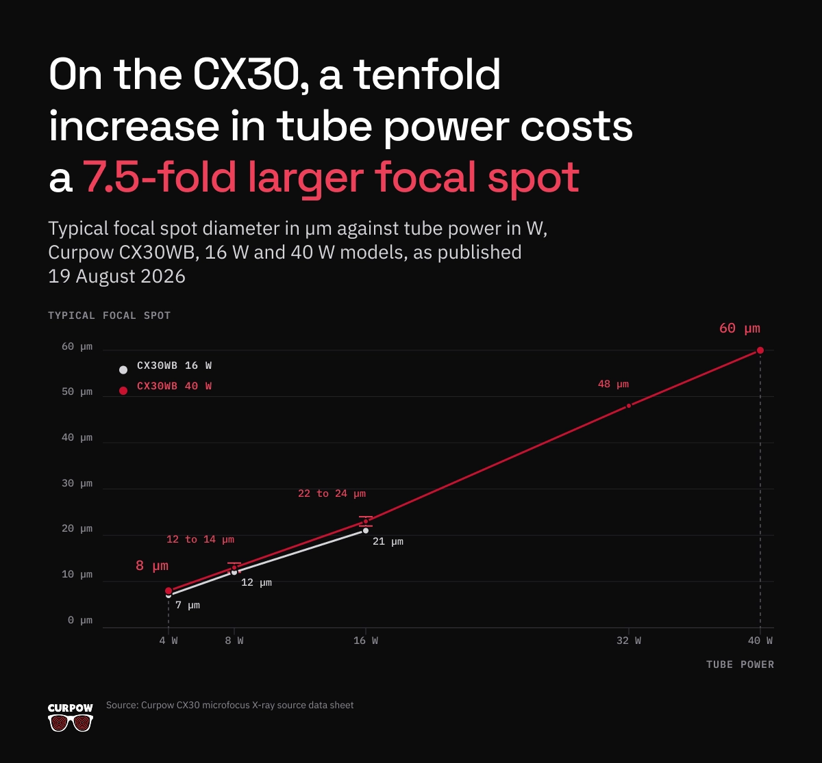
Power rises ten times down the 40 W column, from 4 W to 40 W. Spot diameter rises 7.5 times, from 8 µm to 60 µm. Spot area goes as the square of diameter, so the area grows about 56 times. Power per unit area at the target drops to roughly 18 percent of its 4 W value.
Against the 25.4 µm the method asks a lab to render sharply, that curve splits into three working ranges. At 4 W the CX30 holds 7 to 8 µm, comfortably inside the requirement and fine enough to work on a 15 µm wire. At 16 W the spot reaches 21 to 24 µm, which is the same order as the wire you are trying to measure. At 40 W the spot measures 60 µm, larger than the widest signal bond wire in the catalogue. The top of that curve buys flux for a fast exposure and gives up the resolution counterfeit verification depends on.
So the operating point is a deliberate choice on this application. A screening lab images a small, thin, low attenuation component, so most of the beam reaches the detector and the exposure needs little flux. That argues for the low power end of the curve, where the spot is smallest. When the machine needs the smallest spot available rather than the most flux, the CX40 reaches 4.5 µm on the wide beam variant at 8 W maximum power.
Tube voltage and contrast through the package
Method 2012.7 states the rule directly: the X-ray voltage shall be the lowest consistent with the sensitivity requirements, and shall not exceed 200 kV. Contrast is the first reason to obey it. The image works because silicon, gold, copper and aluminium absorb more than epoxy moulding compound, and raising tube voltage flattens the absorption difference between materials. A lab measuring a die outline against a genuine component is reading a greyscale step at the die edge. Specify more voltage than the component needs and that step gets shallower, until the measurement a screening decision rests on becomes an argument about where the edge sits.
The component is the second reason. A counterfeit screening methodology published by the Center for Advanced Life Cycle Engineering lists X-ray inspection as non-destructive, and records reported instances of part damage from X-ray radiation exposure alongside handling damage such as electrostatic discharge. A lab screening a lot it intends to sell has a commercial reason to work at the low end of the voltage range.
Moulded plastic components sit at the bottom of the voltage range. A few millimetres of epoxy over a silicon die attenuates far less than a battery case or a metal casting. The CX40 tops out at 90 kV on the wide beam variant and 80 kV on the side window variant, which puts its whole range in the band the method points a lab toward.
Voltage headroom matters on the harder packages. Three cases raise the attenuation the beam has to cross. Ceramic hermetic components carry metal lids. Power devices carry heavy copper frames and thick heat slugs. Stacked assemblies put several substrates in one path. For those the CX20 at 110 kV and the CX30 at 130 kV take over. All three sources sit well inside the 200 kV ceiling the method sets.
Tube current and power decide how long an exposure takes. The CX20 runs to 25 W and 250 µA, against the CX40 at 8 W. So it holds a small spot with more flux behind it when a lab has a lot to clear and a deadline. Its data sheet lists high flux and spot location stability, for consistent imaging with minimal variation over time. All three sources use a tungsten (W) target behind a beryllium (Be) window. Beryllium sits at atomic number 4, so it absorbs less than any practical alternative and passes the softer part of the spectrum that builds contrast on a light component.
Beam angle and the extra views the method requires
One view does not finish this inspection. For flat packages, dual in line packages and hybrid packages, Method 2012.7 specifies a first view with the X-rays penetrating in the Y direction. Where a lab needs more than one view, the method puts the second and third views in the Z and X directions. For stud mounted and cylindrical axial lead devices it puts the first view in the X direction. The second and third views go in the Z direction and at 45 degrees between the X and Z directions.
Those extra views exist because a single transmission image projects the whole component onto one plane. Every die, every frame arm and every wire lands on the same pixels. On a stacked package a lab counting wires from one view cannot say which die a wire belongs to. Turn the component, or shoot it off axis, and the layers separate.
Beam angle makes off axis views practical. A wide beam still illuminates the component when the machine tilts it or moves it off the central axis, and a narrow beam runs out of coverage first. How far off axis a given source reaches depends on the beam angle, the focus to object distance and the mechanical layout together, so work it out for your own geometry. The CX40 delivers 108 degrees on the wide beam variant and 40 degrees on the narrow beam. The CX30 delivers a 115 degree round beam with a uniform profile, and its data sheet names that wide round beam as suited to automated inspection and off angle views. The CX20 delivers 125 degrees on the wide beam and 90 degrees on the narrow beam.
Distortion sets the limit on how far off axis a machine can work. Method 2012.7 requires the exposure to hold distortion under 10 percent while still resolving 0.0254 mm. Push the geometry too far off axis and the projected die outline stops being a measurement of the real die outline. So a machine designed for die size comparison needs its off axis angles fixed and repeatable, not left to an operator.
Spot position stability and repeatable comparison
Counterfeit detection is a comparison, and a comparison only holds if the geometry stays put. A lab images a genuine component, then images a suspect component, then measures the difference in die outline and wire placement. If the focal spot moves between those two exposures, the magnification changes and the difference the lab measures includes the source rather than the component.
The CX30 data sheet lists a highly stable spot position, and a high reliability design for in line applications. The CX20 data sheet lists high flux and spot location stability, for consistent imaging with minimal variation over time. Both sources also carry automatic source conditioning, which ramps the source up gradually after a spell switched off, and both expose diagnostics and operating logs over an RS-232 digital interface.
The log matters when a result gets challenged. A customer disputes a screening report and asks whether the equipment was working. The operating log lets your field team answer from records rather than from memory, and it separates a source problem from a detector, fixture or software problem.
Choosing between the CX40, CX20 and CX30 for counterfeit detection
All three sources are low powered and high kV, which is the trade this work wants: enough voltage to cross a package, and a small enough spot to resolve a fine wire.
| Feature | CX40 | CX20 | CX30 |
|---|---|---|---|
| Minimum focal spot | 4.5 µm wide beam, 5 µm narrow, 15 µm side window | 5 µm narrow beam, 7 µm wide beam | 7 µm at 4 W, see FIGURE 1 for the full curve |
| Maximum tube voltage | 90 kV, 80 kV side window | 110 kV | 130 kV |
| Maximum power | 8 W | 25 W | 16 W or 40 W model |
| Tube current | 0 to 180 µA narrow, 0 to 160 µA wide, 0 to 178 µA side window | 0 to 250 µA | 0.320 mA at 16 W, 0.500 mA at 40 W |
| Beam angle | 108° wide, 40° narrow, 34° side window | 90° narrow, 125° wide | 115° round, uniform profile |
| Focus to object distance | 6.0 mm wide beam, 12.0 ± 0.5 mm narrow | 7.5 ± 1.0 mm | 10 ± 0.5 mm spot to window |
| Target and window | Tungsten (W) target, beryllium (Be) window | Tungsten (W) target, beryllium (Be) window | W target, Be window 0.51 mm |
| Weight | 3.6 kg | 5.7 kg | 8.6 kg |
| Input power | 12 to 14 VDC, 4 A max | 24 to 27 V, 4 A max | 24 to 27 V, 7 A max |
| Control interface | RS-232 digital standard on wide beam, analog available | RS-232, digital | RS-232 digital, Windows GUI supplied |
Specifications from the CX40, CX20 and CX30 data sheets. The CX40 data sheet names electronic component inspection including PCBs and semiconductors, automated X-ray inspection and high resolution non-destructive testing among its applications.
The CX40 leads for counterfeit detection. It pairs the smallest focal spot in the range with the shortest focus to object distance. So it reaches the highest geometric magnification on a fine pitch package. Its 90 kV ceiling sits at the low end the method asks for, which is the right end for a moulded plastic body. Its 108 degree wide beam gives it wide off axis coverage, with only the CX20 wider. Its 8 W ceiling costs little on a component this thin.
The CX20 suits a lab clearing volume. It gives up 0.5 µm of spot against the CX40 narrow beam and returns three times the power, which buys exposure time back. Its 110 kV also opens up ceramic and heavier framed components. Its data sheet names component inspection and non-destructive testing directly.
The CX30 suits a machine that also has to handle the hard packages. It carries the voltage for metal lids and thick frames. It publishes the full spot against power curve, so you can pick an operating point deliberately, and it lists a highly stable spot position for comparison work. The CX40 also ships in a side window configuration, which its data sheet offers for compact enclosures, running a 34 degree beam at a 15 µm spot to 80 kV.
Curpow builds these as integrated sources, with tube, high voltage power supply and controller in one package. See the products hub for the full range, and the PCB and electronics inspection page if the same machine also has to inspect assembled boards.
Lead time and second sourcing for screening equipment builders
Curpow designs and manufactures microfocus X-ray sources, high voltage low power X-ray modules and stand alone X-ray power supplies. Those parts go inside the equipment that inspection OEMs and integrators build. Curpow also builds application specific turnkey X-ray inspection systems.
Lead time is six weeks. On a machine build schedule that is often the specification that decides the supplier, because a source that arrives after the frame, the stage and the detector holds up the whole integration. Equipment builders fund second source qualification for that reason, rather than waiting until a supplier misses.
How to specify an X-ray source for counterfeit detection
- Name the measurement, not the application. You can specify against “die outline measured against a genuine reference, and bond wire termination resolved to the individual frame arm”. You cannot specify against “detect counterfeits”.
- Set resolution from the finest wire your customers screen, not from the die. Signal bond wires run from 15 µm upward, and the die outline is a hundred times larger. Work out the smallest wire diameter in the part numbers your customer handles, then allow enough pixels across it to measure a position rather than register a line.
- Take the 25.4 µm figure as the floor and not the goal. MIL-STD-883 Method 2012.7 asks for a sharply defined image of a 0.0254 mm object at less than 10 percent distortion. A machine that only just achieves it has no margin for the finer wires in a modern fine pitch package.
- Ask for focal spot at your operating power, and ask which method measured it. A supplier who can only quote a minimum focal spot has not told you what the source does inside a running machine.
- Decide early how many views you need. Stacked and overmoulded components need off axis views to separate the layers, and that decision drives beam angle and mechanical clearance rather than spot size.
- Fix the hardest package first. A ceramic hermetic component with a metal lid sets the voltage requirement, and a moulded plastic component sets the contrast requirement. Specify for both, because a lab does not get to choose what arrives.
- Specify spot position stability separately from spot size, and ask what the source logs. A comparison against a reference image taken weeks earlier depends on it.
What this means for your source selection
The requirement is already published: render a 25.4 µm feature sharply, hold distortion under 10 percent, work at the lowest tube voltage that penetrates the package, and take more than one view. All four of those land on the source rather than on the detector or the software. So the source decides what a screening machine can conclude, and the finest wire your customers screen is the number that should drive which source you buy.
If you are specifying a source now, send us the smallest package your customers screen, the wire diameter in it, and how many components a shift has to clear. We will tell you which source fits, and at what operating point. Talk to Curpow engineering. Browse our other applications on the applications hub.
Sources
“Radiography”. MIL-STD-883G Method 2012.7, US Department of Defense, method revision dated 1 June 1993; test method standard for microcircuits; full text. Establishes methods, criteria and standards for radiographic examination of semiconductor and hybrid devices, covering equipment requirements, tube voltage selection, required views, radiographic quality standards and the acceptance criteria for internal defects including extraneous matter, wire tails, wire spacing, die attach voids and element mounting.
“Screening for Counterfeit Electronic Parts”. Bhanu Sood and Diganta Das, Center for Advanced Life Cycle Engineering, Department of Mechanical Engineering, University of Maryland, College Park; as originally published in the IPC APEX EXPO Proceedings; conference paper, full text. Presents a systematic methodology for detecting counterfeit parts, covering external visual inspection, marking permanency tests, X-ray inspection, and material evaluation and characterization. Names die size and bond wire alignment as the attributes X-ray verifies, the authentic part image as required equipment, and includes X-ray comparisons of counterfeit and genuine MAX3490EESA components.
“A Lightweight Method for Detecting IC Wire Bonding Defects in X-ray Images”. Daohua Zhan, Jian Lin, Xiuding Yang, Renbin Huang, Kunran Yi, Maoling Liu, Hehui Zheng, Jingang Xiong, Nian Cai, Han Wang and Baojun Qiu. Micromachines, volume 14, issue 6, MDPI, 2023; DOI 10.3390/mi14061119; peer reviewed paper, full text. The authors built an inspection system from an X-ray source, a flat panel detector, a motion control card and a four axis motion platform, running 60 to 80 kV at a 0.5 mm focal spot onto a 92 µm pixel detector, and classified five wire bonding defect types across 800 original X-ray images.
“Bonding Wire: Gold, Silver, Copper, Aluminum”. TopLine Corporation, distributing bonding wire manufactured by Tanaka; product catalogue, current at 2026. Lists 4N gold bonding wire from 15 µm to 50 µm, silver alloy wire from 15 µm to 30 µm, palladium coated copper wire from 15 µm to 50 µm, aluminium with 1 percent silicon from 18 µm to 80 µm, and large diameter power aluminium wire from 100 µm to 600 µm.
“CX40 Microfocus X-Ray Source”, “CX20 Microfocus X-Ray Source” and “CX30 Microfocus X-Ray Source” data sheets, plus the Curpow company page. Curpow Inc.; manufacturer specifications, typical values; CX30 sheet dated 19 August 2026.
FAQ
Direct answers
Frequently asked questions about X-Ray Detection of Counterfeit Electronic Components
What does X-ray inspection detect in a counterfeit electronic component?
X-ray inspection of a counterfeit electronic component detects a package with no die inside, and a die whose outline differs from a genuine component of the same part number. It also detects the wrong number of bond wires, bond wires landing on the wrong lead frame arm, and foreign material sealed inside the body. Screening labs verify die size and bond wire alignment against an X-ray image of a component they know is genuine. X-ray does not resolve the manufacturer markings on the die surface, so it cannot authenticate a component by reading the die itself.
What resolution does counterfeit electronics X-ray inspection need?
Counterfeit electronics X-ray inspection needs a single-digit micrometre focal spot. MIL-STD-883 Method 2012.7 requires radiographic equipment able to render a sharply defined image of an object 0.0254 mm across, which is 25.4 µm, at less than 10 percent distortion. Signal bond wires run from 15 µm to 50 µm in diameter for gold, and 18 µm to 80 µm for aluminium with 1 percent silicon. So the wire rather than the die sets the requirement. The Curpow CX40 reaches a 4.5 µm focal spot on its wide beam variant.
Why is a 25.4 µm feature the published requirement for X-raying a component?
25.4 µm is one mil, and one mil is the standard diameter of a signal bond wire in a microelectronic package. MIL-STD-883 Method 2012.7 requires the equipment focal distance and the exposure to render a sharply defined image of an object with a major dimension of 0.0254 mm. The method also rejects a foreign particle greater than 0.025 mm and a bond smaller than 0.025 mm, so the same dimension recurs through its acceptance criteria. MIL-STD-883 wrote its requirement around the bond wire.
What tube voltage does X-ray inspection of electronic components need?
Moulded plastic components sit at the bottom of the voltage range, because a few millimetres of epoxy moulding compound absorbs far less than a metal case. MIL-STD-883 Method 2012.7 requires the X-ray voltage to be the lowest consistent with the sensitivity requirements and caps it at 200 kV. Ceramic hermetic components with metal lids, power devices with heavy copper lead frames, and stacked packages raise the requirement toward 110 kV or 130 kV. Raising voltage beyond what a component needs flattens the contrast between the silicon die and the epoxy around it.
Why does focal spot size change with tube power on an X-ray source?
The focal spot is the area where the beam current lands on the target, and the target has a thermal limit, so more power has to spread over more area. The Curpow CX30WB 40 W data sheet shows the effect directly: a typical focal spot of 8 µm at 4 W becomes 60 µm at 40 W. Ten times the power gives 7.5 times the spot diameter and about 56 times the spot area. A single minimum focal spot figure therefore says little about what a source delivers inside a running inspection machine.
Can a standard automated X-ray inspection system verify a component is genuine?
A standard automated X-ray inspection system finds gross wire faults and cannot verify authenticity. Researchers ran an X-ray source with a 0.5 mm focal spot at 60 to 80 kV, onto a detector with a 92 µm pixel. That system classified high loop, low loop, broken, missing and sagging bond wires reliably. A 0.5 mm focal spot measures roughly 20 times a signal bond wire diameter, which is enough to see that a wire is absent or badly shaped. Measuring a die outline against a genuine reference, and resolving which lead frame arm each wire terminates on, needs a microfocus source.
Which Curpow source suits counterfeit electronics X-ray inspection?
The CX40 leads. Its wide beam variant carries a 4.5 µm focal spot and a 6.0 mm focus to object distance, the shortest in the Curpow range. So it reaches the highest geometric magnification on a fine pitch package, and its 108 degree beam gives the machine room to work off axis. The CX40 data sheet names electronic component inspection including PCBs and semiconductors. The CX20 offers a 5 µm narrow beam spot at 110 kV with 25 W behind it, which shortens exposures on high volume screening. The CX30 reaches 130 kV for ceramic and heavily framed components, and it publishes a full focal spot against tube power curve.