Electronics inspection · Application note
X-Ray Sources for PCB and Electronics Inspection
- Published 13 October 2026
- 19 min read
- Curpow application engineering
Short answer
PCB inspection needs a single-digit micrometre focal spot, enough magnification to size voids, and a beam wide enough for off-angle views. The CX40 leads with a 4.5 µm spot and a 6.0 mm focus to object distance. The CX20 adds power and the CX30 reaches 130 kV.
On this page
- What X-ray inspection finds on a PCB assembly
- BGA, chip scale, QFN and through hole: what changes for the source
- In-line AXI, off-angle views and offline CT
- What resolution a PCB inspection machine needs
- Focal spot size at your operating power
- Tube voltage and contrast through an electronics assembly
- Spot position stability for computed tomography of packages
- Choosing between the CX40, CX20 and CX30 for electronics inspection
- Lead time and second sourcing for inspection machine builders
- How to specify an X-ray source for an inspection machine
- What this means for your source selection
- Sources
On a circuit board, the connections that hold a chip in place sit underneath the chip. Each one is a small ball of solder, and a single chip can have hundreds of them. Once the chip goes down, nobody can see any of them again. So electronics manufacturers use an X-ray machine to look through the chip and check that every connection formed properly.
IPC publishes the standards that electronics manufacturers inspect against. Those standards define how much empty space a solder ball may contain, and where inside the joint that space is allowed to sit. A machine working from a single image can measure the size but not the location. We checked the CX40, CX20 and CX30 against what those criteria ask of a source. So you can read the acceptance requirement and our specifications in the same place.
Inspection machine builders use X-ray to measure voiding inside solder balls, find bridges and opens under the package, confirm barrel fill on through holes, and check bond wires inside a part. Four things decide whether an X-ray source can do that work. Focal spot size at the power the machine runs. Enough magnification to put the feature across enough pixels. A beam wide enough to shoot off-angle. Spot position stability, if the machine reconstructs. This page works through each one.
Key takeaways
- X-ray is the only method that reaches a joint sitting under the package. BGA, chip scale and bottom termination packages hide every connection beneath the body. Optical inspection stops at the package edge, and electrical test reports that a net conducts today rather than that a joint will survive thermal cycling.
- Void acceptance runs by product class, and where the void sits changes the answer. Published work applying IPC-7095A on a lead-free line treated a void of 12 percent or larger at the interconnection interface as unacceptable for a Class 2 product. Class 3 work in aerospace and defence carries tighter limits again.
- Void location decides a joint, not void size alone. Voids at the ball to package and ball to pad interfaces leave less solder carrying the load. They also put an air gap in the heat path. Voids enclosed inside the ball body matter less at the same diameter.
- A machine looking straight down cannot tell you where a void sits. It has to judge every void by the harshest interface criterion, which fails good boards. Off-angle views recover the location, and beam angle is the source specification that makes them possible.
- Set resolution from the smallest void you must size, not from the ball. A void covering 9 percent of a joint by area measures 30 percent of that joint across. On a 0.45 mm joint that is a feature near 135 µm. Microvoids sit far below it.
- The CX40 leads this work in the Curpow range. It carries the smallest focal spot at 4.5 µm and the shortest focus to object distance at 6.0 mm. Its data sheet names electronic component inspection including PCBs and semiconductors.
What X-ray inspection finds on a PCB assembly
A finished assembly hides most of its own joints, and taking it apart destroys it. So inspection machine builders use X-ray instead. It finds five kinds of defects:
- Voiding inside the solder joint. Gas trapped during reflow leaves empty space inside the ball. IPC-7095 separates these by mechanism rather than lumping them together. It names macrovoids, planar microvoids, shrinkage voids, microvia voids, intermetallic compound microvoids and pinhole voids as distinct classes. Each class sits at a different size and a different place in the joint. So one void percentage limit does not describe the problem on its own.
- Opens, head-in-pillow and non-wet joints. A ball that touched the paste but never merged with it looks joined from outside and carries no reliable connection. The ball keeps its own outline instead of collapsing into a single mass, and X-ray shows that outline. Electrical test can pass a head-in-pillow joint that opens later under vibration or thermal cycling.
- Bridging and stray solder. Excess solder between two adjacent balls shorts them. On a fine pitch device the gap between neighbouring joints is smaller than the joints themselves. So the machine has to resolve a small bridge across an even smaller gap.
- Plated through hole barrel fill. Wave and selective soldering push solder up through a barrel, and the acceptance question is how far up it climbed. The beam crosses the full board thickness here rather than a package body. So barrel fill sets a different attenuation path from every other defect on this list.
- Internal package faults. Wire bonded packages run fine wires from the die to the substrate under the overmold. The assembly process can leave those wires swept, shorted to a neighbour or lifted. Die attach voiding sits in the same category. Machines that verify a part matches its marking work from these same internal structures. That subject belongs on our counterfeit electronics detection page.
| Feature | Reported dimension | What was measured, and when | What it does not show |
|---|---|---|---|
| Solder mask opening on a PBGA land | 0.40 to 0.50 mm | Plastic BGA packages at 0.8 mm and 1.0 mm ball pitch, one manufacturer’s application report, 2009 revised 2015 | Ball diameter after reflow, and any pitch below 0.8 mm |
| Solder pad copper on the same substrate | 0.60 to 0.65 mm | Same packages | Land geometry on chip scale or bottom termination parts |
| Minimum trace and space | 0.05 mm | Same substrates, 2 and 4 layer designs | The finest geometries available on advanced substrates today |
| Via diameter | 0.2 mm | Same substrates | Microvia diameters, which run smaller |
| Substrate thickness | 0.56 ± 0.04 mm at 2 layers, 0.61 ± 0.05 mm at 4 layers | Same substrates | Finished board thickness, which the beam also has to cross |
| Void screening threshold in a lead-free study | 9 percent by area, equal to 30 percent by diameter | 229 balls carrying voids, drawn from three 736-pin BGAs on each of 10 assemblies at one contract manufacturer, 2006 | An IPC limit. This was the screening threshold above which those 229 balls got measured further |
Package and substrate dimensions from the Texas Instruments PBGA application report; the void screening threshold from work presented at IPC APEX 2006. Full references at the foot of the page.
BGA, chip scale, QFN and through hole: what changes for the source
Package type decides two things a source cares about: how small the smallest joint is, and how much material the beam crosses to reach it.
| Package type | Where the connections sit | What that means for the source |
|---|---|---|
| Plastic BGA, 0.8 to 1.0 mm pitch | A grid of solder balls under the package body, on lands with a 0.40 to 0.50 mm solder mask opening | The largest joints on the assembly, and the easiest case. Moderate magnification puts a whole joint across enough pixels to measure a void area against it |
| Fine pitch and chip scale packages | Balls under a package barely larger than the die itself, at pitches well below 0.8 mm | The smallest joints, and the gap between neighbours shrinks with the joints. Magnification decides whether the machine can measure at all, so a short focus to object distance matters more here than anywhere else on the board |
| QFN and bottom termination components | Flat metallised pads under the body, with no ball and no standoff | There is no ball outline to measure a void against, so the void area gets judged against the pad. Voiding under a thermal pad is a heat path problem rather than a mechanical one |
| Plated through hole | A barrel running through the full board | The attenuation path is board thickness plus copper, not a package body. This is the case that pushes tube voltage up rather than resolution down |
| Wire bonded packages | Fine wires from the die to the substrate, sealed under the overmold | The finest features on the assembly, and the reason a machine specified only for BGA work often cannot do component level inspection |
Package construction and substrate figures per the Texas Instruments PBGA application report. Pitch conventions vary by manufacturer, so confirm the smallest package on your customer’s board before you specify the machine around it.
In-line AXI, off-angle views and offline CT
IPC-7095 treats these as separate inspection techniques rather than one method at different speeds. Its contents list transmission X-ray, computed tomography and automated X-ray inspection under their own headings. The difference that matters to a machine builder is what each one can say about a void.
A transmission system takes one exposure straight down through the package. That is fast enough to inspect every assembly coming off the line. The image shows that a void exists and how large it measures in projection. It cannot tell you where that void sits. Every layer of the joint lands on the same pixel.
A system inspecting only from above has to evaluate every void against the interface criterion. That rejects joints which would have passed on their merits. Moving the X-ray source for an off-angle view changes that. Shoot across the joint rather than through it, and the void separates from the interfaces in the image. A system with off-angle capability can judge a void by its real location.
Laminography and computed tomography slice the joint properly and give the location outright. They also cost scan time no production line can spend on every assembly. Use them for failure analysis and process qualification, not for screening.
| Method | What it establishes | What was reported, and when | What it does not show |
|---|---|---|---|
| Transmission, straight down | Void presence and projected void area against ball area | Study of 229 voided balls at one contract manufacturer, 2006 | Where the void sits. The study reports that a transmission system inspecting from above must evaluate all voids against the interface criterion regardless of true location |
| Transmission, off-angle | Whether a void sits within the ball or at an attachment interface | Same 229 balls, on transmission systems able to move the X-ray source | Full three dimensional void geometry, which needs reconstruction |
| Laminography or CT | Void location by layer, resolved within the ball and at both interfaces | Same 229 balls, on a laminography system run alongside the transmission system | Anything at line rate. Reconstruction time rules it out for screening every assembly |
All three rows from work presented at IPC APEX 2006, comparing a laminography system against a transmission system on the same voided balls.
Beam geometry is the source specification that buys the off-angle view. The CX40 puts out a 108 degree wide beam. The CX30 puts out a 115 degree round beam with a uniform profile. Its data sheet describes that beam as suited to automated inspection and off-angle views. A narrow beam limits how far off-axis the machine can work before the field of view runs out.
What resolution a PCB inspection machine needs
PCB and electronics inspection runs on a single-digit micrometre focal spot. The features that decide a joint run from roughly 130 µm down to a few micrometres, and focal spot size sets the floor under all of them.
Start from the void you have to size. Void diameter scales as the square root of void area. So a void covering 9 percent of a joint by area measures 30 percent of that joint across. On a plastic BGA land with a 0.40 to 0.50 mm solder mask opening, that puts you on a feature roughly 120 to 150 µm across. Measuring its area accurately enough to argue about a percentage limit takes tens of pixels across it, not three.
Smaller features sit below that. IPC-7095 names planar microvoids and intermetallic compound microvoids as classes of their own, separate from macrovoids, and both sit well below the macrovoid scale. Minimum trace and space on a plastic BGA substrate run 0.05 mm, and the wires inside a wire bonded package are finer again. A machine specified only against the largest joint on the board cannot see the features that fail in service.
The spot is an area rather than a point, so every projection carries some blur. At the detector that blur is the focal spot size multiplied by (M − 1), where M is the geometric magnification. Referred back to the object, it becomes F(1 − 1/M), which approaches the focal spot size and never exceeds it. So above about 5× magnification you are within 20 percent of F, and the spot rather than the geometry is what limits you.
Magnification is the other half. Getting the board close to the spot is what makes magnification available. So focus to object distance decides how much of it a machine can reach. A 4.5 µm spot at a 6.0 mm focus to object distance resolves more on a fine pitch package than a smaller spot held further away.
Curpow’s range sits at the small end of that requirement. The CX40 reaches 4.5 µm on the wide beam variant and 5 µm on the narrow beam. The CX20 reaches 5 µm narrow beam and 7 µm wide beam, with 25 W behind it. The CX30 starts at 7 µm and publishes how the spot grows as tube power rises.
A focal spot number is a measurement result, not a physical dimension. ASTM E2903-18 covers effective focal spots from 5 to 300 µm at up to 225 kV, measured by radiographs of edges. PTB’s NanoXSpot project, run under the European metrology programme precisely because this gap exists, states that manufacturers use proprietary measurement methods that give inconsistent results. Ask which method produced the number before you compare two data sheets.
Focal spot size at your operating power
Tube power drives focal spot size. The spot is where the beam current lands on the target, and the target has a thermal limit. More power has to spread over more area. That means a data sheet quoting a minimum focal spot and a maximum power output is quoting two numbers that do not occur together.
Curpow publishes the full relationship on the CX30 rather than a single best-case figure. A machine builder needs the spot at the power their throughput demands, and only a curve gives that.
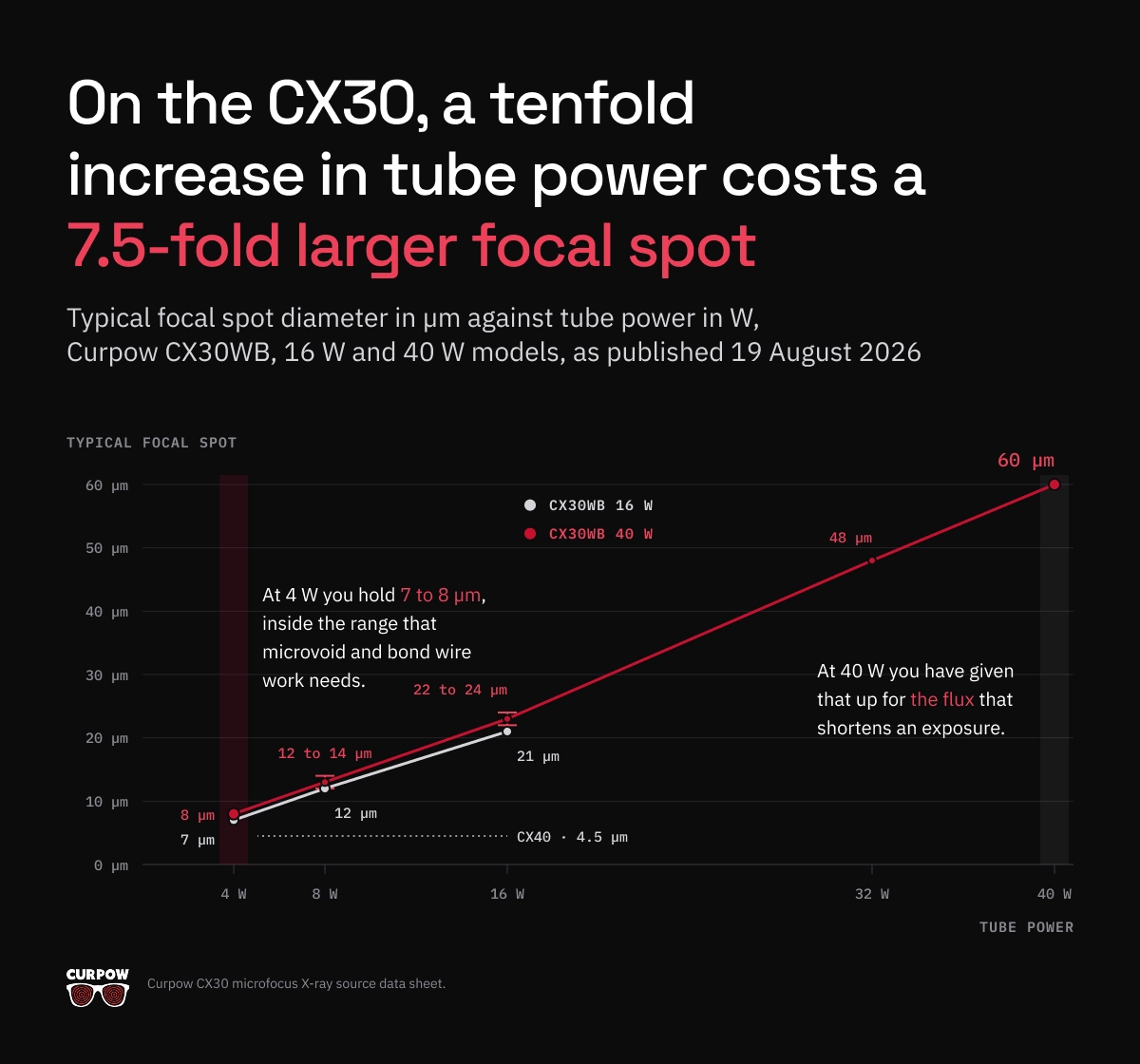
Read down the 40 W column and the shape of the trade is clear. Power rises ten times, from 4 W to 40 W. Spot diameter rises 7.5 times, from 8 µm to 60 µm. Spot area goes as the square of diameter, so the area grows about 56 times. Power per unit area at the target drops to roughly 18 percent of its 4 W value.
That trade decides where a machine lands. At 4 W you hold 7 to 8 µm, inside the range that microvoid and bond wire work needs. At 40 W you have given that up for the flux that shortens an exposure. Both are valid operating points for an inspection machine, and the throughput your customer specified decides which one you buy.
When the machine needs the smallest spot rather than the most flux, the CX40 reaches 4.5 µm on the wide-beam variant, at 8 W maximum power.
Tube voltage and contrast through an electronics assembly
Board assemblies rarely need high tube voltage. A populated board is thin and mostly low atomic number material. The beam crosses far less attenuating mass than a battery case or a metal casting. The CX40 tops out at 90 kV on the wide-beam variant and 80 kV on the side-window, and that clears most bare and populated boards.
Metal in the beam path changes that. A heat spreader or lid sits directly over the package. A shielding can covers a whole RF section. Heavy copper planes on a power board raise attenuation across the board rather than locally. Stacked and package-on-package assemblies put two or more substrates and their solder in a single path. In those cases the CX20 at 110 kV and the CX30 at 130 kV take over.
Contrast pulls the other way. Raising kV improves penetration and flattens the attenuation difference between solder and the substrate underneath it. On a thin assembly you can specify more voltage than the job needs and lose the contrast that makes a void edge measurable. A void is empty space inside solder, so the measurement rests on the greyscale step at the void boundary. Check what contrast a source leaves you at the joint, not just whether it penetrates the package.
Tube current and power carry the other half of image quality. The CX20 runs to 25 W and 250 µA, against the CX40 at 8 W. So it holds a small spot with more flux behind it when cycle time tightens. Its data sheet lists high flux and spot location stability, for consistent imaging with minimal variation over time.
Spot position stability for computed tomography of packages
If your machine reconstructs a package rather than screening a board, spot position stability belongs in the specification next to spot size. Drift during a scan smears every projection that follows, and a stable 8 µm spot will out-reconstruct an unstable 5 µm one every time.
The CX30 data sheet lists a highly stable spot position for CT and 3D work, and a high reliability design for in-line applications. The CX20 sheet lists high flux and spot location stability. Both also carry automatic source conditioning, which ramps the source up slowly after a spell switched off. Both expose diagnostics and operating logs over an RS-232 digital interface.
A customer reports that void measurements have drifted. The operating log is what lets your field team tie that drift back to the source. Without it the reflow profile, the detector and the algorithm all stay suspects.
Choosing between the CX40, CX20 and CX30 for electronics inspection
All three are low powered and high kV by design, which is the right trade for solder joint and package work.
| CX40 | CX20 | CX30 | |
|---|---|---|---|
| Minimum focal spot | 4.5 µm wide beam, 5 µm narrow, 15 µm side-window | 5 µm narrow beam, 7 µm wide beam | 7 µm at 4 W, see FIGURE 1 for the full curve |
| Maximum tube voltage | 90 kV, 80 kV side-window | 110 kV | 130 kV |
| Maximum power | 8 W | 25 W | 16 W or 40 W model |
| Tube current | 0 to 180 µA narrow, 0 to 160 µA wide, 0 to 178 µA side-window | 0 to 250 µA | 0.320 mA at 16 W, 0.500 mA at 40 W |
| Beam angle | 108° wide, 40° narrow, 34° side-window | 90° narrow, 125° wide | 115° round, uniform profile |
| Focus to object distance | 6.0 mm wide beam, 12.0 ± 0.5 mm narrow | 7.5 ± 1.0 mm | 10 ± 0.5 mm spot to window |
| Target and window | Tungsten (W) target, beryllium (Be) window | Tungsten (W) target, beryllium (Be) window | W target, Be window 0.51 mm |
| Weight | 3.6 kg | 5.7 kg | 8.6 kg |
| Input power | 12 to 14 VDC, 4 A max | 24 to 27 V, 4 A max | 24 to 27 V, 7 A max |
Specifications from the CX40, CX20 and CX30 data sheets. The CX40 data sheet names electronic component inspection including PCBs and semiconductors, automated X-ray inspection and high-resolution non-destructive testing among its applications.
The CX40 combines the smallest spot in the range with the shortest focus to object distance. So it reaches the highest magnification on a fine pitch package. The CX20 trades 0.5 µm of spot for three times the power, which buys exposure time back. The CX30 carries the voltage and the published spot against power curve. Specify it when a machine has to handle shielded assemblies or reconstruct a package.
The CX40 also ships in a side-window configuration, which its data sheet offers for compact enclosures. That variant runs a 34 degree beam at a 15 µm spot, to 80 kV.
Lead time and second sourcing for inspection machine builders
Curpow designs and manufactures microfocus X-ray sources, high voltage low power X-ray modules and stand-alone X-ray power supplies. Those go inside the equipment that inspection OEMs and integrators build. Curpow also builds application-specific turnkey systems.
Lead time is six weeks. On a machine build schedule that is often the specification that matters most, because a source that arrives after the frame and the detector holds up the whole integration. Machine builders fund second-source qualification for that reason rather than deferring it until a supplier fails.
How to specify an X-ray source for an inspection machine
- Name the measurand, not the application. You can specify against “void area as a percentage of joint area on a 0.4 mm pitch chip scale package, with void location resolved to interface or body”. You cannot specify against “inspect the board”.
- Start from the smallest package your customer runs, not the typical one. Fine pitch chip scale packages and wire bonded parts set the resolution requirement. You cannot upgrade a machine built around 1.0 mm pitch BGAs without changing the source.
- Set resolution from the smallest void you must size. A void at 9 percent by area is 30 percent of the joint across. Work out that dimension for your smallest joint, then allow enough pixels across it to measure an area rather than detect a blob.
- Fix the product class and the void criteria before the machine design. Class 2 and Class 3 work carry different limits, and IPC-7095 lets a manufacturer and its customer agree criteria for the end use. The number your customer inspects to decides the resolution the machine needs.
- Decide early whether you need void location. If you do, the machine needs off-angle capability, and that means beam angle and mechanical clearance, not just a smaller spot.
- Ask for focal spot at your operating power, and ask which standard measured it. If a supplier cannot give you a spot against power curve, you do not yet know what the source does in your duty cycle.
- If the machine reconstructs, specify spot position stability separately from spot size, and ask what the source logs.
What this means for your source selection
The joints that decide whether an assembly survives sit underneath the parts, and nothing else reaches them on a finished board. Customers write their acceptance criteria in void percentages, and only an X-ray image measures those. The bridges, the barrel fill and the bond wires come free with the same station.
If you are specifying a source now, send us the smallest package on your customer’s board, the acceptance standard you are building to, and your cycle time. We will tell you which source fits, and at what operating point. Talk to Curpow engineering. Browse our other applications on the applications hub.
Sources
“Acceptability of Electronic Assemblies”. IPC-A-610J, IPC International, Bannockburn, Illinois, April 2024; consensus standard covering visual quality acceptability requirements for electronic assemblies, including a surface mount area array voids section.
“Design and Assembly Process Guidance for Ball Grid Arrays (BGAs)”. IPC-7095E, IPC International, Bannockburn, Illinois, August 2024, superseding IPC-7095D-WAM1 of June 2019; developed by the Ball Grid Array Task Group (5-21f) of the Assembly and Joining Committee (5-20); consensus standard. Carries separate sections on X-ray inspection, X-ray image acquisition, transmission X-ray and computed tomography, automated X-ray inspection, voids in BGA solder joints by class, void measurement and sampling plans for void evaluation.
“X-ray Inspection of Voids in BGA Joints with Respect to the IPC-7095A Specification”. Rajiv Balsavar, Agilent Technologies, Loveland, Colorado; presented at IPC Printed Circuits Expo, APEX and the Designers Summit, 2006, paper S16-02; conference paper with the author’s own experimental work; full text. The study covered 229 voided balls drawn from three 736-pin BGAs on each of 10 assemblies at a single contract manufacturer, with 10 balls sectioned to confirm the X-ray measurements.
“Plastic Ball Grid Array (PBGA)”. Application report SSZA002B, Texas Instruments, August 2009, revised August 2015; manufacturer application report; full text. Describes cavity-up laminate PBGA packages from 17 mm to 35 mm square at 0.8 mm and 1.0 mm ball pitch with 208 to 976 balls, and lists nominal substrate dimensions including solder mask opening, solder pad copper, trace and space, via diameter and substrate thickness.
“Standard Test Method for Measurement of the Effective Focal Spot Size of Mini and Micro Focus X-ray Tubes”. ASTM E2903-18, ASTM International, 2018, reapproved 2024; consensus standard; cited for its published scope, which covers focal spot dimensions from 5 to 300 µm on systems up to and including 225 kV tube voltage by means of radiographs of edges, and draws on EN 12543-5. Focal spots larger than 300 µm fall under E1165 instead.
“18NRM07 NanoXSpot: Traceable measurement of focal spot size and shape”. Physikalisch-Technische Bundesanstalt, under the EMPIR programme co-financed by participating states and Horizon 2020; project record, 2019; national metrology institute project documentation.
“CX40 Microfocus X-Ray Source”, “CX20 Microfocus X-Ray Source” and “CX30 Microfocus X-Ray Source” data sheets, plus the Curpow company page. Curpow Inc.; manufacturer specifications, typical values; CX30 sheet dated 19 August 2026.
FAQ
Direct answers
Frequently asked questions about X-Ray Sources for PCB and Electronics Inspection
What defects does X-ray inspection find on a PCB assembly?
X-ray finds voiding inside solder joints, opens and head-in-pillow joints, bridging between adjacent joints, incomplete barrel fill on plated through holes, and internal package faults. A head-in-pillow joint is one where the ball touched the paste but never merged with it. Internal package faults include swept or shorted bond wires and die attach voiding. IPC-7095 separates solder joint voids into macrovoids, planar microvoids, shrinkage voids, microvia voids, intermetallic compound microvoids and pinhole voids. Those classes sit at different sizes and different places inside the joint.
How much voiding is acceptable in a BGA solder joint?
That depends on the product class and on where the void sits. Published work applying IPC-7095A on a lead-free line treated a void of 12 percent or larger at the interconnection interface as unacceptable for a Class 2 product. The contract manufacturer and its customer tightened the within-ball figure from 20 percent to 17.5 percent by area for that product. Class 3 work in aerospace and defence carries tighter limits than Class 2, and IPC-7095 also lets a manufacturer and its customer agree criteria for the end use.
What focal spot size does PCB X-ray inspection need?
A single-digit micrometre spot, which is why these machines use microfocus sources. A void covering 9 percent of a joint by area measures 30 percent of that joint across. A plastic BGA land has a solder mask opening of 0.40 to 0.50 mm, which puts that void near 135 µm. Microvoids and the wires inside a wire bonded package sit far below it. Focal spot size sets the resolution floor, because blur referred back to the object approaches the spot size and never exceeds it. The Curpow CX40 reaches 4.5 µm on the wide beam variant.
Why can a 2D X-ray image not tell you where a void sits in a solder ball?
A single transmission image projects the whole joint onto one plane, so the ball body and both attachment interfaces land on the same pixel. A comparison of a laminography system against a transmission system, run on 229 voided balls taken from 736-pin BGAs, found that the transmission system had to evaluate every void against the interface criterion whatever its true location. Moving the source for an off-angle view separates the interfaces from the ball body and recovers the location.
How much tube voltage does PCB X-ray inspection need?
90 kV clears the large majority of assemblies. A populated board is thin and mostly low atomic number material, so the beam crosses little attenuating mass. Voltage becomes the deciding specification when a heat spreader, a shielding can, heavy copper planes or a stacked package adds metal to the beam path. Those cases call for 110 kV or 130 kV. Derive it from the thickest orientation of your customer’s worst assembly, then check the contrast that voltage leaves at the joint.
Why does focal spot size change with tube power?
The spot is where the beam current lands on the target, and the target has a thermal limit, so more power spreads over more area. The CX30WB 40 W data sheet shows it directly: a typical spot of 8 µm at 4 W becomes 60 µm at 40 W. Ten times the power, 7.5 times the diameter, 56 times the area. A single minimum focal spot figure says little about what a source does inside a running inspection machine.
Which Curpow source suits a PCB inspection machine?
The CX40 leads. Its wide-beam variant carries a 4.5 µm focal spot and a 6.0 mm focus to object distance, the shortest in the range. The CX40 data sheet names PCB and semiconductor inspection directly. The CX20 offers a 5 µm narrow beam spot at 110 kV and 25 W, which buys exposure time back when cycle time tightens. The CX30 reaches 130 kV, publishes a full spot against power curve, and lists a highly stable spot position for CT and 3D work.